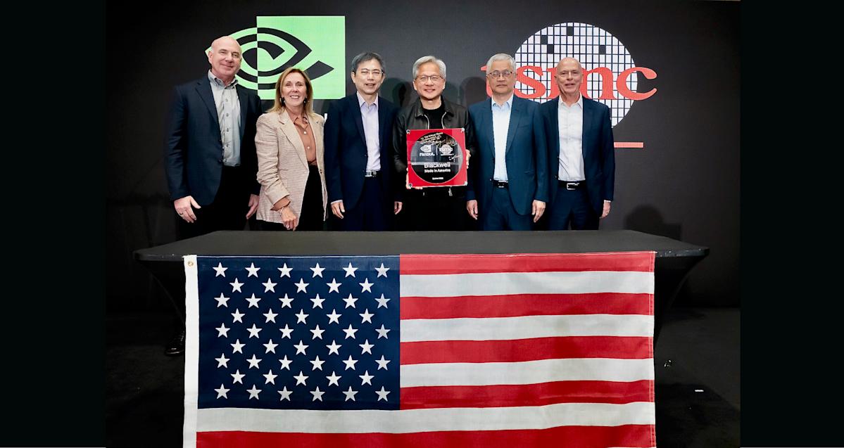
NVIDIA Unveils First U.S.-Made Blackwell Wafer at TSMC Phoenix Facility
Key Points
- NVIDIA produced its first Blackwell wafer at TSMC’s Phoenix, Arizona fab.
- The wafer serves as the base material for NVIDIA's next‑gen AI chips.
- Blackwell offers up to 25× lower cost and energy use versus previous chips.
- Major AI firms such as Amazon, Google, and OpenAI have pledged to use Blackwell.
- CEO Jensen Huang highlighted the milestone as a historic U.S. manufacturing achievement.
- Domestic production aims to reduce exposure to tariffs and geopolitical risks.
- NVIDIA plans to expand U.S. manufacturing footprint and invest heavily in AI infrastructure.
- A half‑trillion‑dollar investment plan involves partnerships with TSMC, Foxconn, and others.
NVIDIA announced the production of its first Blackwell wafer at TSMC’s Phoenix, Arizona fab, marking a major step in domestic chip manufacturing for its AI hardware. The Blackwell platform, touted as more powerful and up to 25 times more cost‑ and energy‑efficient than its predecessor, is positioned for volume production and aims to strengthen ties with major AI players while reducing exposure to tariffs and geopolitical risks. CEO Jensen Huang highlighted the significance of the milestone for U.S. semiconductor leadership and noted ongoing plans to expand U.S. manufacturing capacity and invest heavily in AI infrastructure.
NVIDIA's Domestic Manufacturing Milestone
NVIDIA revealed that the first Blackwell wafer, the foundational material for its next‑generation AI chips, has been assembled at Taiwan Semiconductor Manufacturing Company’s (TSMC) advanced semiconductor manufacturing facility in Phoenix, Arizona. This development represents a pivotal move toward bolstering domestic chip production for the company’s flagship AI hardware.
The Blackwell Platform's Advancements
The Blackwell architecture, introduced by NVIDIA last year, is designed to reshape the AI industry. It promises significantly higher performance while delivering up to 25 times lower cost and energy consumption compared to the previous generation of NVIDIA AI chips. Major AI developers, including Amazon, Google, and OpenAI, have already committed to adopting the architecture, underscoring its industry‑wide relevance.
Strategic Implications and Leadership Commentary
CEO Jensen Huang emphasized the historic nature of the achievement, stating that it is “the very first time in recent American history that the single most important chip is being manufactured here in the United States by the most advanced fab, by TSMC.” By producing Blackwell wafers domestically, NVIDIA aims to insulate its supply chain from evolving tariff regimes and geopolitical tensions, enhancing resilience and strategic autonomy.
With the Blackwell platform now ready for volume production, NVIDIA is actively pursuing the expansion of its manufacturing footprint across the United States. Earlier in the year, the company announced plans to channel half a trillion dollars into building AI infrastructure in the U.S. through collaborations with TSMC, Foxconn, and other partners, reinforcing its commitment to domestic innovation and capacity building.
Future Outlook
The successful fabrication of the Blackwell wafer in Phoenix signals a broader shift toward on‑shore semiconductor manufacturing for high‑performance AI workloads. NVIDIA’s continued investment and partnership strategy is poised to accelerate the deployment of advanced AI technologies while supporting U.S. leadership in the global semiconductor ecosystem.