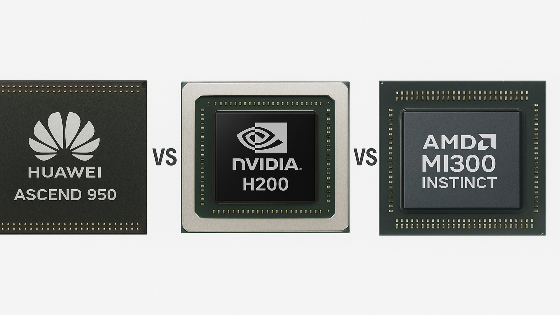
Huawei Ascend 950, Nvidia H200, and AMD MI300 Instinct: Head‑to‑Head AI Chip Comparison
Key Points
- Huawei Ascend 950 uses a proprietary AI accelerator on a 5 nm process.
- Nvidia H200 (GH100 Hopper) and AMD MI300 both run on 5 nm nodes.
- Transistor counts: H200 ~80 billion; MI300 ~153 billion; Ascend 950 undisclosed.
- Memory bandwidth peaks at 6.55 TB/s for AMD, 4.89 TB/s for Nvidia, and 4 TB/s for Huawei.
- FP8 performance: Ascend 950 targets 1 PFLOP, Nvidia H200 reaches 2 PFLOPs.
- FP16 performance ranges from 241 TFLOPs (Huawei) to 383 TFLOPs (AMD).
- All chips use PCIe 5.0 x16 and are offered in server‑grade cards.
- Target workloads include LLM training, inference, and high‑performance computing.
- Availability timelines differ: Nvidia early 2023, AMD already shipping, Huawei Q4 2026.
A side‑by‑side look at three leading AI accelerators—Huawei's Ascend 950 series, Nvidia's H200 (GH100 Hopper), and AMD's Radeon Instinct MI300 (Aqua Vanjaram). The comparison covers architecture, process technology, transistor counts, die size, memory type and capacity, bandwidth, compute performance across FP8, FP16, FP32 and FP64, and target scenarios such as large‑scale LLM training, inference, and high‑performance computing. Availability timelines differ, with each vendor positioning its chip for data‑center and HPC workloads.
Architecture and Process
Huawei’s Ascend 950 series uses a proprietary AI accelerator architecture built on a 5 nm process. Nvidia’s H200 is based on the Hopper GPU architecture, also fabricated on a 5 nm node. AMD’s MI300 employs the CDNA 3.0 architecture, again on a 5 nm process.
Transistor Count and Die Size
The Ascend 950’s transistor count has not been disclosed, while the H200 contains roughly 80 billion transistors and the MI300 about 153 billion. Die sizes differ: the H200’s die is approximately 814 mm², and the MI300’s is about 10 mm²; Ascend 950’s die size is not specified.
Memory Subsystem
Huawei integrates its own HiZQ 2.0 proprietary HBM, delivering 4 TB/s bandwidth. Nvidia pairs the H200 with HBM3e, offering about 4.89 TB/s. AMD equips the MI300 with HBM3, reaching roughly 6.55 TB/s. Memory capacities are 144 GB for Ascend 950, 141 GB for H200, and 128 GB for MI300, with bus widths of 6144‑bit (Huawei) and 8192‑bit (Nvidia); AMD’s bus width is not listed.
Compute Performance
In FP8 (or MXFP8/HiF8) the Ascend 950 targets 1 PFLOP, while the H200 reaches 2 PFLOPs. MI300’s FP16 performance is around 383 TFLOPs, with FP32/FP64 combined at about 47.87 TFLOPs. The Ascend 950 provides 241.3 TFLOPs FP16, 60.3 TFLOPs FP32, and 30.2 TFLOPs FP64. Nvidia’s H200 delivers 600 W TDP and features 16,896 CUDA cores, 528 fourth‑gen Tensor cores, and 14,080 shaders with 220 compute units and 880 Tensor cores.
Form Factor and Connectivity
All three chips are offered in server‑grade cards or SuperPoD configurations and use PCIe 5.0 x16 interfaces. Power envelopes are around 600 W for Nvidia; Huawei and AMD power specifications are not detailed.
Target Scenarios and Availability
Huawei positions the Ascend 950 for large‑scale training and decode inference of LLMs and generative AI. Nvidia’s H200 targets AI training, HPC, and data‑center workloads. AMD’s MI300 focuses on AI/HPC compute acceleration. Release windows vary, with Nvidia’s H200 slated for early 2023, Huawei’s Ascend 950 aimed at Q4 2026, and AMD’s MI300 already available.